ADC USING SUCCESSIVE-APPROXIMATION
A successive approximation ADC
is a type of analog-to-digital converter that converts a continuous
analog waveform into a discrete digital representation via a binary
search through all possible quantization levels before finally
converging upon a digital output for each conversion.
BLOCK DIAGRAM:
 | |||||
| Fig 1: Successive Approximation ADC Block Diagram |
Block Explanation:
- A sample and hold(S/H) circuit to acquire the input voltage (Vin).
- An analog voltage comparator that compares Vin with the output of the internal DAC and the result of the comparison outputs is given to the successive approximation register (SAR).
- A successive approximation register subcircuit designed to supply an approximate digital code of Vin to the internal DAC.
- An internal reference DAC that, for comparison with V, supplies the comparator with an analog voltage equal to the digital code output of the SARin.
Using
741 om-amp to do the comparator operation, the op-amp contain two input
one is inverter i/p(-) and another is non inverter i/p(+) see (fig 2),
 | |||||
| fig 2: Comparator. |
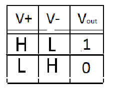
It compares two voltages or currents and outputs is digital logic as show in table. It has two analog input terminals  and
and  and one binary digital output
  . The output is ideally( either high or low),
and and one binary digital output . The output is ideally( either high or low), 
DAC
DAC which convert digital to equivalent analog voltage by using R2R ladder technique as show in fin 3.
 | ||||
| Fig 3: DAC |
OPERATION OF SUCCESSIVE APPROXIMATION ADC
The
operation of SAR is quite different, we see the example of 3 bit ADC
this method applicable for all n bit. It execute step by step depend
upon clock frequency.
For n bit code each bit have some voltage level with respect to reference voltage here i give 3 bit ADC. so we get three voltage level as show in figure 4,
For n bit code each bit have some voltage level with respect to reference voltage here i give 3 bit ADC. so we get three voltage level as show in figure 4,
 |
| Fig 4: |
EXAMPLE 1:
To convert the give 5v analog voltage from sensor into relevant 3 bit digital value using SAR ADC method, the full scale value is 8V.ANSWER:
CONSIDER:
INPUT FULL SCALE: 8VNO OF BIT O/P: 3bits
INPUT VOLTAGE: 5V
The number of bit is 3 so the sampling of signal is 2 ^n we get 8 level of sampling
First ADC starts conversation on receiving signal high to low(0 to 1) at START pin.
when this signal will received, SAR (successive approximation register) is initialized so that the most significant bit (MSB) is equal to a digital 1 and remind zero {" 1 0 0 (D2 D1 D0) "} as show in fig5
 |
| Fig 5 |
This code is fed into the DAC, then DAC convert to equalent analog voltage of this digital code (Vref/2 of D2(MSB) remaining everything is zero show in figure 4.
DAC get code( 1 0 0) from SAR then convert in to equivalent analog voltage(Vref) from our example we get value the value 4 using R2R ladder method as show in fig 6,
D2 D1 D0 Data from SAR when stat
1 0 0
4 * 0 2 * 0 1 * 0 Equivalent voltage in DAC using R2R ladder
4 + 0 + 0 = 4 Output from DAC( given to comparator as Vref)
fig 6
fig 6
That Vref is given to comparator. The comparator compare the voltage from Vref(DAC) and Vin(sensor) if Vref<Vin o/p is 1 else 0,


Output of comparator is given to SAR. Then SAR produce another code depend upon output of the comparator given below
if comparator o/p is 1 SAR o/p is 0 0 0
comparator o/p is 0 SAR o/p is 1 1 0
which means when comparator value is one the SAR will hold the last value and generate the next bit high.
If it low, it will low the last bit MSB and high the next bit
Now the SAR output is give to DAC that and change to relevant analog voltage
D2 D1 D0 Data from SAR when stat
1 1 0
4 * 1(D2) 2 * 1 1 * 0 Equivalent voltage in DAC using R2R ladder
4 + 2 + 0 = 6 output from DAC( given to comparator as Vref)
fig 8
That Vref is given to comparator. The comparator compare the voltage from Vref(DAC) and Vin(sensor) if Vref<Vin o/p is 1 else 0,
Here the output is 0 because(Vref>Vi/p).
Comparator output is given to the SAR that produce another code depend upon output of the comparator given below
if comparator o/p is 1 SAR o/p is 1 1 1
comparator o/p is 0 SAR o/p is 1 0 1
which means when comparator value is one the SAR will hold the last value and generate the next bit high.
If it low, it will low the last bit MSB and high the next bit given below
fig 8
That Vref is given to comparator. The comparator compare the voltage from Vref(DAC) and Vin(sensor) if Vref<Vin o/p is 1 else 0,
Here the output is 0 because(Vref>Vi/p).
 |
| Fig 9 |
if comparator o/p is 1 SAR o/p is 1 1 1
comparator o/p is 0 SAR o/p is 1 0 1
which means when comparator value is one the SAR will hold the last value and generate the next bit high.
If it low, it will low the last bit MSB and high the next bit given below
 |
| Fig 10. |
Now DAC produce analog voltage
comparator compare Vref and Vi/p. Here the output is 1 because(Vref < Vi/p).
After comparing the three times the SAR hold the last vlaue which is given see in above fig 11.
the output of 5V analog is 1 0 1
D2 D1 D0 Data from SAR when stat
1 0 1
4 * 1(D2) 2 * 0 (D1) 1*0(D0) Equivalent voltage in DAC using R2R ladder
4 + 0 + 1 = 5 Output from DAC( given to comparator as Vref)
this 5 volt given to comparator
this 5 volt given to comparator
comparator compare Vref and Vi/p. Here the output is 1 because(Vref < Vi/p).
 |
| Fig 11. |
the output of 5V analog is 1 0 1
No comments:
Post a Comment