#include <REGX51.H>
#include<LCD.c>
sbit EOC=P3^0; // End Of Conversion;
sbit STR=P3^1; // Start;
sbit OE=P3^2; // Output Enable;
sbit ALE=P3^3; // Address Latch Enable;
void adc_con(unsigned char);
void main()
{
P1=0XFF;
OE=0;
ALE=0;
STR=0;
EOC=1;
ini();
address(0x80);
string("adc:");
while(1)
{
ALE=1;
STR=1;
ALE=0;
STR=0;
while(EOC==0);
OE=1;
adc_con(P1);
OE=0;
}
}
void adc_con(unsigned char a)
{
unsigned char c1,c2,c3;
address(0x85); // address of the LCD display
c1=(a/100)+48;
c2=((a%100)/10)+48;
c3=a%10+48;
write(c1); // write value to lcd display
write(c2);
write(c3);
}
Saturday, 28 December 2013
Interfacing ADC 0808 with 8051 using proteus
Interfacing ADC 0808 with 8051
I/O Pin Details
Analog Channel Selection
ADC 0808 have 8 different channel. For proper channel selection logic as per table is provided to Pin no. 23, 24,25.

Reference Voltage or Step Size
Step Size or Reference voltage can be calculated from equation Step Size = (VREF(+) + VREF(-))/2 If we consider VREF(-) = Gnd and VREF(+) = 5V then step size = 5/256 = 19.53 mV. If you using temperature sensor LM35 then step size is 10 mV. 10 mV step size can be set by VREF(-) = Gnd and VREF(+) = 2.56V.
ALE
ALE (Address Latch Enable) is L - to H pulse to latch in address.
START
ADC starts conversation on receiving this signal high to low. Successive approximation register (SAR) is reset on the positive edge of the start conversion (SC) pulse. The conversion is begun on the falling edge of the start conversion pulse.
EOC (End Of Conversion)
This is an active low O/P signal from ADC on receiving low EOC micro controller Come to know that the converted data is ready to be picked up.
OE (Output Enable)
ADC converts the analog input to its binary equivalent and holds it in an internal register. L- to-H OE is used to enabling TRI - STATE output, so Converted data can be red from data pin D0 – D7.
Clock signal
Clock signal cannot be faster then 100ms.It can be external or provided from microcontroller crystal using 4 D- F/F as frequency divider. Single D- F/F divides frequency by 2.
Signal conditioning
If sensor signal is very low then apply proper amplification. You need simple opam amplifier. Normally sensor O/P is in range of mV and affected by noise very easily for better accuracy apply 2 - 5 gain. If you using temperature sensor LM35 its O/P is 10mv/C and it is advised to amplification by gain of 2 – 5.
Circuit Diagram
 |
| Fig 1: ADC simulation interface with AT89c51. |
Simulation timing diagram
 |
| Fig 2: Simulation timing diagram |
Algorithm to program the ADC 0808 through AT89C51
- Connect the ADC as shown in diagram. Provide Clock signal from micro controller crystal by step down its frequency with help of D – F/F
- Select the analog channel. If necessary apply proper signal conditioning as mentioned.
- Provide Low to High transition on ALE to latch in the address
- Provide Low to High transition on SC to let ADC to initiate converting from selected analog channel to equivalent digital bit.
- Now monitor for EOC signal from ADC to high to low. H- to-L EOC indicates that data is ready to collect.
- Now finally make OE L- to-H to read data from internal buffer

If you want code click here
ADC USING SUCCESSIVE-APPROXIMATION TECHNIQUE
ADC USING SUCCESSIVE-APPROXIMATION
A successive approximation ADC
is a type of analog-to-digital converter that converts a continuous
analog waveform into a discrete digital representation via a binary
search through all possible quantization levels before finally
converging upon a digital output for each conversion.
BLOCK DIAGRAM:
 | |||||
| Fig 1: Successive Approximation ADC Block Diagram |
Block Explanation:
- A sample and hold(S/H) circuit to acquire the input voltage (Vin).
- An analog voltage comparator that compares Vin with the output of the internal DAC and the result of the comparison outputs is given to the successive approximation register (SAR).
- A successive approximation register subcircuit designed to supply an approximate digital code of Vin to the internal DAC.
- An internal reference DAC that, for comparison with V, supplies the comparator with an analog voltage equal to the digital code output of the SARin.
Using
741 om-amp to do the comparator operation, the op-amp contain two input
one is inverter i/p(-) and another is non inverter i/p(+) see (fig 2),
 | |||||
| fig 2: Comparator. |
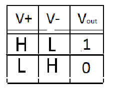
It compares two voltages or currents and outputs is digital logic as show in table. It has two analog input terminals  and
and  and one binary digital output
  . The output is ideally( either high or low),
and and one binary digital output . The output is ideally( either high or low), 
Analog to Digital Convertor(ADC)
Analog-to-digital converter
An analog-to-digital
converter (abbreviated ADC, A/D or A to D) is a device
that converts a continuous physical quantity (usually voltage) to a digital
number that represents the quantity's amplitude(An
analog signal is continuous in both time and amplitude, whereas a digital
signal is discrete in time as well as in amplitude).
 |
| Fig:1 Analog to digital conversion |
In most of the digital system needs to take
input from Analog sensor or transducer. Analog signal are most common input
signal for embedded system. Sensor or transducer Such as Temperature, Motion,
pressure, Humidity are analog.
SAMPLING AND QUANTIZATION
The basic way to convert the analog signal into digital signal by using sampling and quantization techniques
which is show in fig:2,

Logically, an ADC has to covert an analog signal to an equivalent digital one in two steps: converting the analog signal to a discrete in time signal and converting it into a discrete in amplitude signal. The process of converting an analog signal to discrete in time signal is called as ‘sampling’ and the process of converting it to a discrete in amplitude signal is called ‘quantization’. These processes can occur in any order.
 |
| Fig:3 sampling and quantisation |
The important parameters consider in ADC is
- Resolution
- Sample rate
- Error rate
- A direct-conversion ADC or flash ADC
- A successive-approximation ADC
- Dual-slope or multi-slope ADC
- A delta-encoded ADC
Subscribe to:
Posts (Atom)